We invite you to the next Solid State Physics seminar.
When: 26 November, Wednesday at 16:30 in room Beijing-1, Moscow School of Management
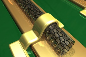
What: Computational Approach to Electrical Contacts in Graphene and Carbon Nanotube Transistors
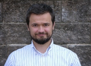
Speaker: Prof. Vasiliy Perebeinos, Skoltech
Abstract: Electrical properties of low-dimensional devices are dominated by the contact resistance. For carbon nanotube field effect transistors (CNT-FETs) [1], as for graphene [2] and MoS2 transistors, the electrical contacts are a key factor limiting device performance. Contact resistance reflects a complex interplay of many factors.
With advances in scaling, the contact resistance and transfer length are becoming even more critical. We have developed a general purpose CNT device simulator which is unique in including quantum-mechanical tunneling, both acoustic and optical-phonon scattering, as well as the crucial transfer of carriers between the CNT and metal contact.
CNT-FETs integration requires closely-spaced arrays of tubes, with several tubes per device, to give adequate drive current. We find that with scaling of the tube spacing toward smaller pitch, there is a structural transition to a geometry in which the metal poorly wets the nanotube and substrate. This gives a sudden decrease in contact adhesion, and probably also an increase in contact resistance. Several interesting aspects of the wetting geometry will be discussed [3].
[1] V. Perebeinos, J. Tersoff, W. Haensch, Phys. Rev. Lett. 111, 236802, (2013). [2] F Xia, V. Perebeinos, Y Lin, Y Wu, P Avouris Nature Nano 6, 179 (2011). [3] V. Perebeinos, J. Tersoff Nano Lett. 14, 4376 (2014).* The Skolkovo Institute of Science and Technology (Skoltech) is a private graduate research university in Skolkovo, Russia, a suburb of Moscow. Established in 2011 in collaboration with MIT, Skoltech educates global leaders in innovation, advances scientific knowledge, and fosters new technologies to address critical issues facing Russia and the world. Applying international research and educational models, the university integrates the best Russian scientific traditions with twenty-first century entrepreneurship and innovation.
* The Skolkovo Institute of Science and Technology (Skoltech) is a private graduate research university in Skolkovo, Russia, a suburb of Moscow. Established in 2011 in collaboration with MIT, Skoltech educates global leaders in innovation, advances scientific knowledge, and fosters new technologies to address critical issues facing Russia and the world. Applying international research and educational models, the university integrates the best Russian scientific traditions with twenty-first century entrepreneurship and innovation.
If you like to participate and for further information or questions, please Liliya Abaimova
Please confirm your attendance. We look forward to seeing you.


