Сколтех — новый технологический университет, созданный в 2011 году в Москве командой российских и зарубежных профессоров с мировым именем. Здесь преподают действующие ученые, студентам дана свобода в выборе дисциплин, обучение включает работу над собственным исследовательским проектом, стажировку в индустрии, предпринимательскую подготовку и постоянное нахождение в международной среде.

Архив метки: semiconductor

New ultra-thin semiconductor could become an alternative to graphene in the next-generation electronics

Following a decade of intensive research into graphene and two-dimensional materials a new semiconductor material shows potential for the future of super-fast electronics.

The new semiconductor named Indium Selenide (InSe) is only a few atoms thick, similarly to graphene. The research was reported in Nature Nanotechnology this week by researchers of The University of Manchester and their colleagues at The University of Nottingham.

Graphene is just one atom thick and has unrivalled electronic properties, which has led to widely-publicized suggestions about its use in future electronic circuits.

For all its superlative properties graphene has no energy gap. It behaves more like a metal rather than a normal semiconductor, frustrating its potential for transistor-type applications.

The new research shows that InSe crystals can be made only a few atoms thick, nearly as thin as graphene. InSe was shown to have electronic quality higher than that of silicon which is ubiquitously used in modern electronics.

Importantly, unlike graphene but similar to silicon, ultra-thin InSe has a large energy gap allowing transistors to be easily switched on and off, allowing for super-fast next-generation electronic devices. Combining graphene with other new materials, which individually have excellent characteristics complementary to the extraordinary properties of graphene, has resulted in exciting scientific developments and could produce applications as yet beyond our imagination.

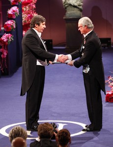
Andre Geim (left) receives the Nobel Prize in Physics

Andre Geim (left) receives the Nobel Prize in Physics

Andre Geim, one of the authors of this study and a recipient of the Nobel Prize in Physics for research on graphene, believes that the new findings could have a significant impact on development of future electronics.

“Ultra-thin InSe seems to offer the golden middle between silicon and graphene. Similar to graphene, InSe offers a naturally thin body, allowing scaling to the true nmanometer dimensions. Similar to silicon, InSe is a very good semiconductor.”

The Manchester researchers had to overcome one major problem to create high-quality InSe devices. Being so thin, InSe is rapidly damaged by oxygen and moisture present in the atmosphere. To avoid such damage, the devices were prepared in an argon atmosphere using new technologies developed at the National Graphene Institute.

This allowed high-quality atomically-thin films of InSe for the first time. The electron mobility at room temperature was measured at 2,000 cm2/Vs, significantly higher than silicon. This value increases several times at lower temperatures.

Current experiments produced the material several mmicrometers in size, comparable to the cross-section of a human hair. The researchers believe that by following the methods now widely used to produce large-area graphene sheets, InSe could also soon be produced at a commercial level.

Ultra-thin InSe is one of a growing family of two-dimensional crystals that have a variety of useful properties depending on their structure, thickness and chemical composition.

Currently, research in graphene and related two-dimensional materials is the fastest growing field of materials science that bridges science and engineering.

Anastasia Turnina, one of the authors, the winner of the Science Drive program, that was organized in Skoltech in 2014 (Anastasia was awarded by 2 year internship in Andre Geim group in the University of Manchester):” We have developed a really promising material. Besides, it is a golden mean according to electrical characteristics and it also demonstrates stabile photoluminescence signal. It is very interesting to work in Andre Geim’s team. Firstly, ideas and projects are very exiting. Secondly, everyone is so experienced and hardworking, so you have study all the time to be on a par.”

The results of the study have been published in Nature Nanotechnology

Контакты:
Skoltech Communications
+7 (495) 280 14 81
Seminar: The Next Life of Silicon

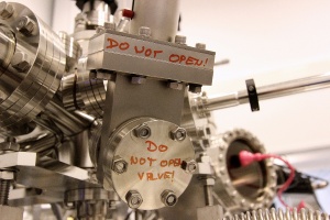
Scanning tunneling microscope. Photo: Ilan Goren

Scanning tunneling microscope. Photo: Ilan Goren

We are pleased to invite to a seminar titled “The Next Life of Silicon” with guest speaker Prof. Gabriel Aeppli (ETH Zürich and EPF Lausanne; head of the Synchrotron and Nanotechnology department of the Paul Scherrer Institute, Switzerland).

Who: Prof. Gabriel Aeppli

When: April 20, 2015 13.30 – 15.00

Where: Beijing-2 auditorium, China cluster Skolkovo School of Management

SEMINAR ABSTRACT:

The 20th century has been distinguished by the silicon-based information revolution, where bits are encoded as charges which are manipulated and stored via field effect transistors. The continued exponential growth of information technology based on straightforward extrapolations of this paradigm is not guaranteed, and there has therefore been a search for both alternative paradigms and materials.

The new paradigms entail exploitation of spin and orbital degrees of freedom, including related quantum phenomena.  While “exotic” materials have been successfully used to demonstrate some of the associated physics, we show here that silicon may be an excellent host for the new effects. In particular, laser cooling and electromagnetic traps have led to a revolution in atomic physics, yielding dramatic discoveries ranging from Bose-Einstein condensation to quantum control of single atoms. Because it is a semiconductor of extraordinary cleanliness which can be acquired at low cost, silicon can also be thought of as a poor man’s atom trap.

We describe here the beginnings of the science of silicon as atom trap, where the trapped atoms are the donor impurities. Key tools, enabling the visualization and manipulation of the impurity quantum states, are free electron lasers and scanning tunneling microscopes.

References:
Greenland et al., Nature (2010)

http://www.nature.com/nature/journal/v465/n7301/full/nature09112.html

Vinh et al., PRX (2013)

http://prx.aps.org/abstract/PRX/v3/i1/e01101

Morley et al, Nature Materials (2010 and 2013)

http://www.nature.com/nmat/journal/v9/n9/full/nmat2828.html and

http://www.nature.com/nmat/journal/v12/n2/full/nmat3499.html

Schofield et al., Nature Comm. (2013) http://www.nature.com/ncomms/journal/v4/n4/full/ncomms2679.html

Prof. Gabriel Aeppli, ETH Zurich and EPFL, guest speaker at the Skoltech seminar

Prof. Gabriel Aeppli, ETH Zurich and EPFL, guest speaker at the Skoltech seminar

SPEAKER INTRODUCTION:

Gabriel Aeppli is professor of physics at ETH Zürich and EPF Lausanne, and head of the Synchrotron and Nanotechnology department of the Paul Scherrer Institute, Switzerland. After taking his B.Sc., M.Sc. and PhD in Electrical Engineering from MIT, he spent the majority of his career in industry (NEC, AT&T and IBM) where he worked on problems ranging from liquid crystals to magnetic data storage.

He was subsequently co-founder and director of the London Centre for Nanotechnology, Quain Professor at University College London, and cofounder of the Bio-Nano Consulting Company. He is a frequent advisor to numerous private and public entities worldwide (including China, Australia, Europe and the US) engaged in the funding, evaluation and management of technology.

A member of the American Academy of Arts and Sciences and Fellow of the Royal Society (London), he was a recipient of the Mott Prize of the Institute of Physics(London), the Oliver Buckley prize of the American Physical Society and the Neel Medal/International Magnetism Prize. His current technical focus is on the implications of photon science and nanotechnology for information processing and health care.

Контакты:
Skoltech Communications
+7 (495) 280 14 81
masterpas_01_icom_small.png
Оплата на сайте

Оплата на сайте

2011-2024 © Сколтех
Сколковский институт науки и технологийСведения об образовательной организации
?>