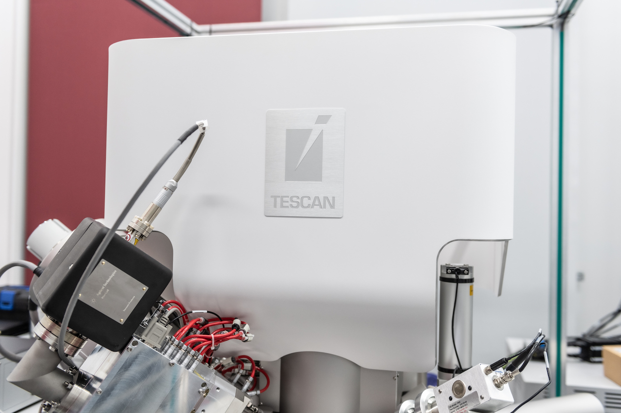
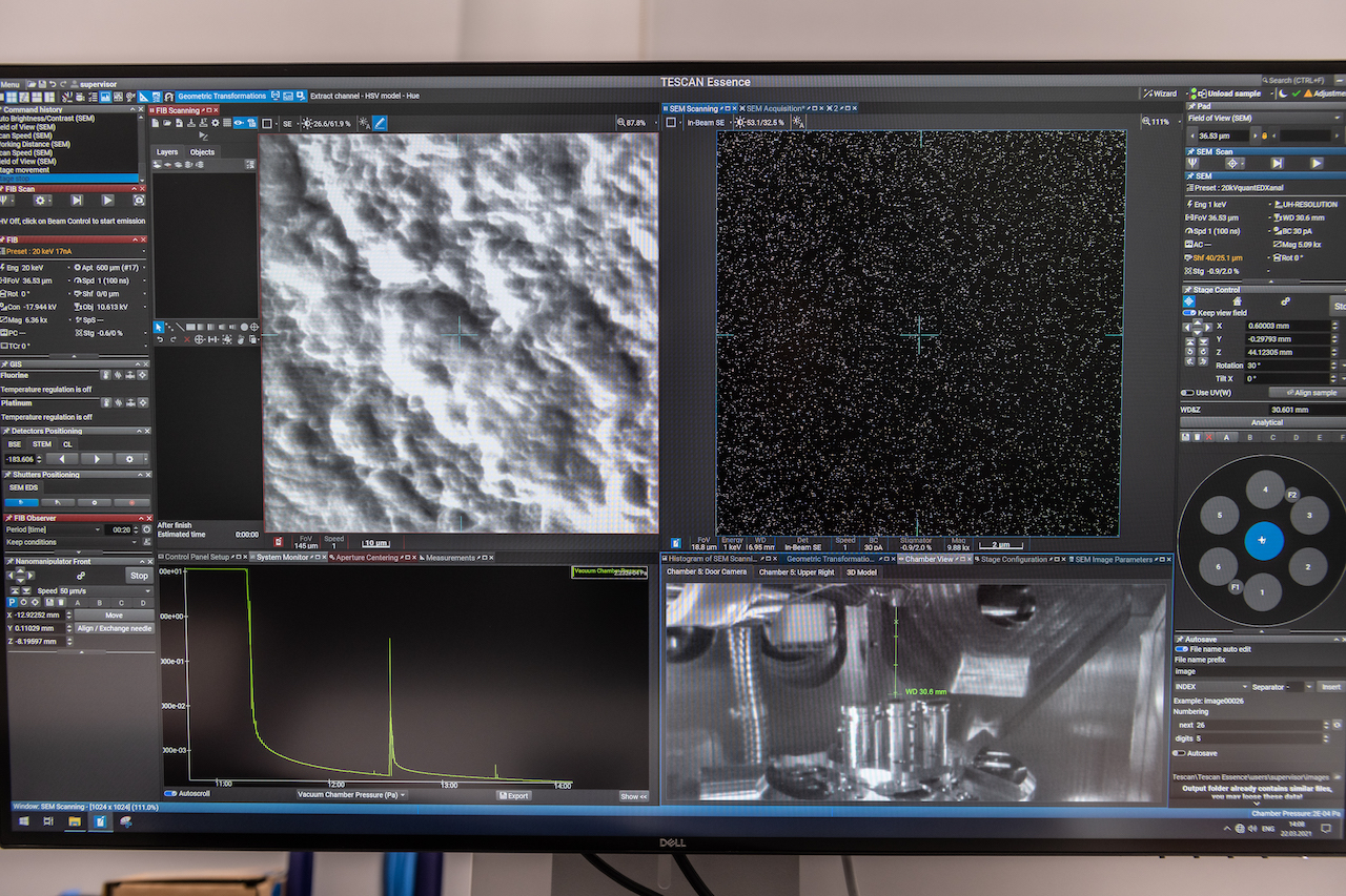
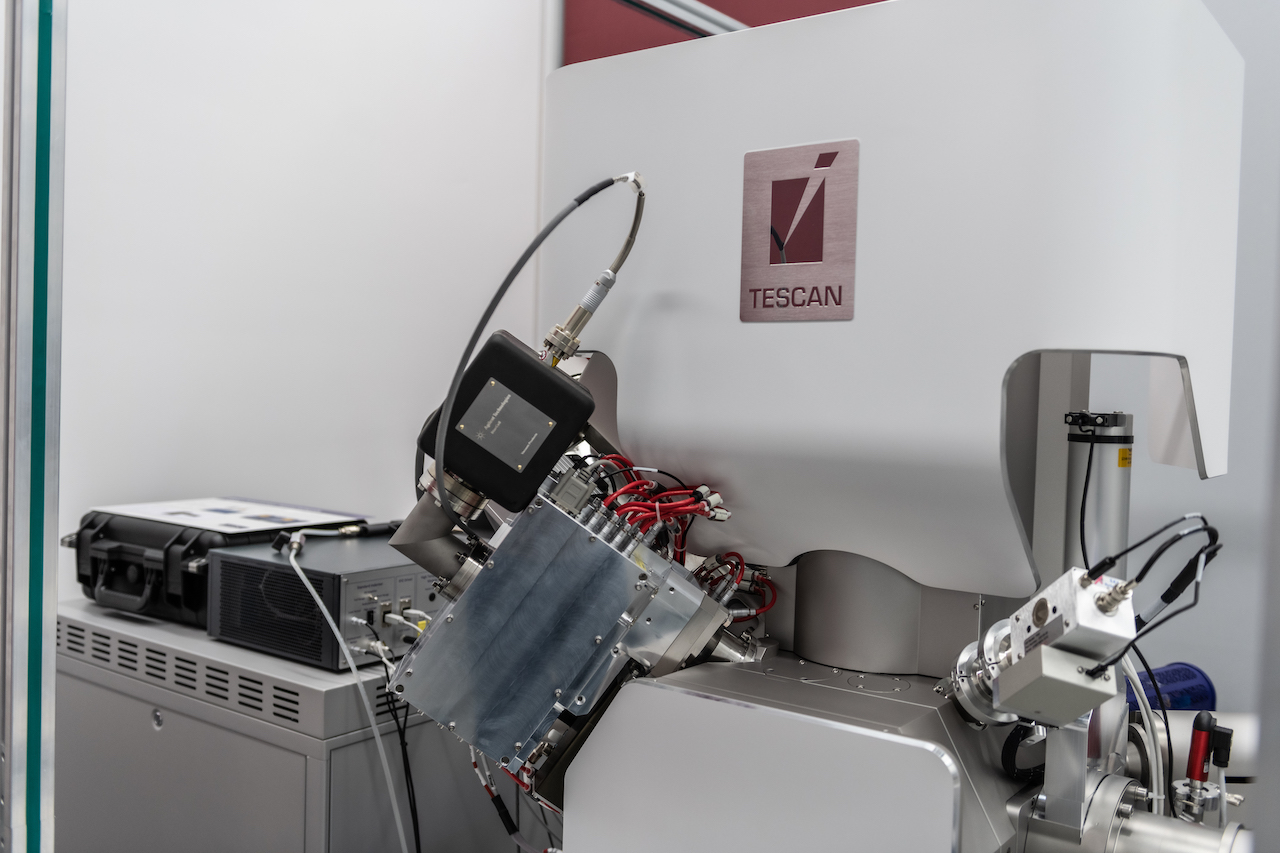
Tescan Solaris, a new focused ion beam-scanning electron microscope (FIB-SEM) will help solve the most challenging tasks lying at the intersection of nano-mechanics and nano-ionics. FIB-SEM technology uses a combination of two focused beams, an electron beam and an ion beam, along with new generation immersion optics, TOF-SIMS mass spectrometry, and nano-indentation technologies. The ion beam can operate as a nanoscale jigsaw to cut out the tiniest micro-samples for nano-mechanical testing, as well as to cause spallation of secondary ions from the material surface that are captured by the time-of-flight detector sensitive to the charge/mass ratio for composition and isotope analysis at the nanoscale in surface layers and nanoparticles, among other things.
“The new device is not just a microscope but a fully fledged nanoscale laboratory for advanced studies in all fields of science, ranging from materials engineering and energy storage to mineralogy, nano-photonics, and biology,” says Skoltech professor Alexander Korsunsky, who proposed and designed the configuration of this new machine.
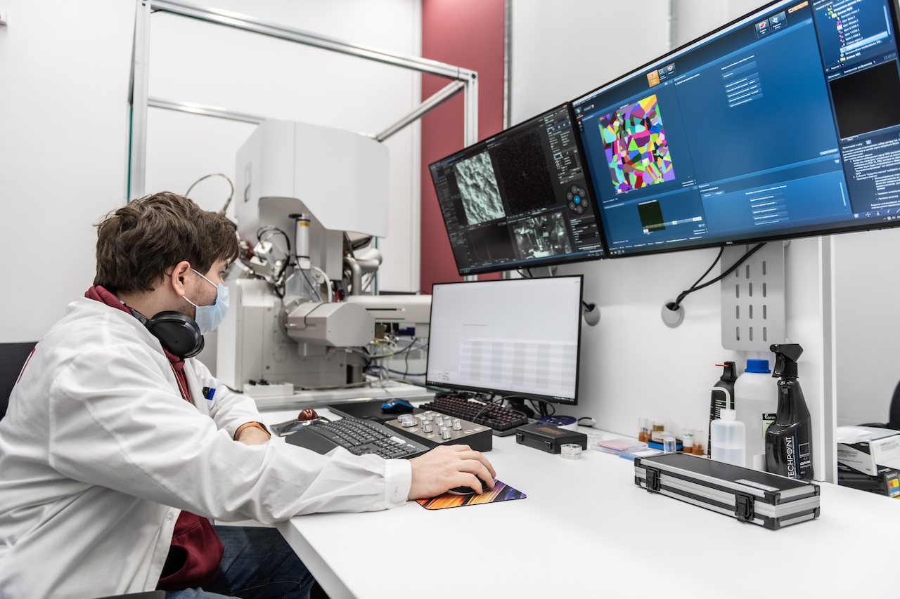
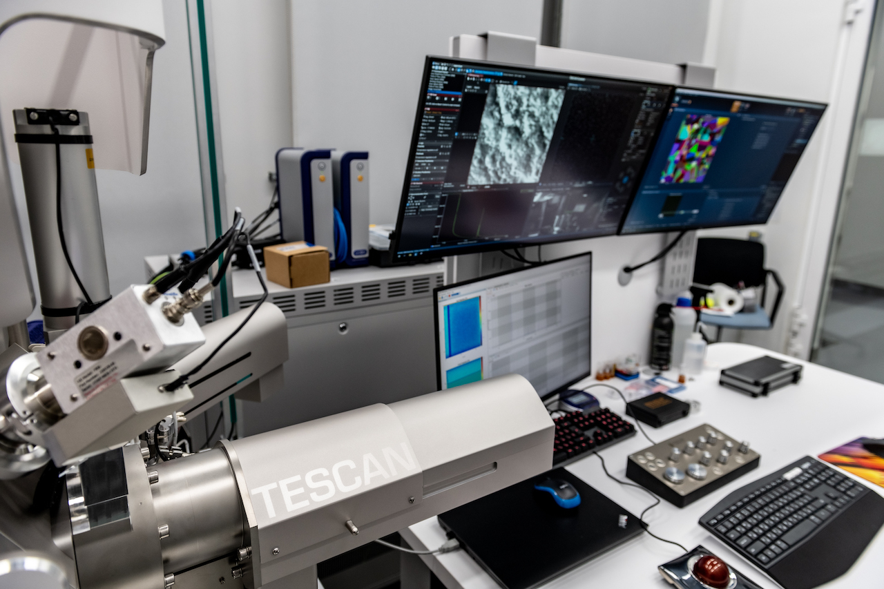
Director of the Advanced Imaging Core facility (AICF) Yaroslava Shakhova says: “This device is the fourth microscope to be installed at AICF. Two are scanning electron microscopes, including one dual-beam SEM that uses xenon as an ion source, and one is a transmission electron microscope (TEM). Having several electron microscopes at our disposal, we can address a broad spectrum of tasks in materials science and beyond. In particular, we can study the morphology of surfaces or particles using SEM or visualize a sample’s cross-section using a dual-beam SEM, for example, when we study the porosity of materials or multilayer structures. The TEM is highly useful for studying materials at a qualitatively different level, for example, for visualizing a material’s crystal lattice or its defects. Importantly, with this microscope, we can investigate atomic-resolution elemental composition using EDX or EELS techniques. Recently, AICF has installed another dual-beam SEM, Tescan Solaris, which uses gallium as an ion source. It is a very useful feature when it comes to preparing samples for high-precision TEM.”
According to professor Korsunsky, a leading expert in materials science and nano-mechanics, Tescan Solaris offers a wealth of new possibilities: “For example, we will be able to visualize cross-sections of lithium batteries using the ion beam and observe the motion of lithium ions using mass spectrometry techniques. This will help to understand some of the most fundamental aspects of the charge and discharge processes that until now could only be assessed using indirect indicators. We will thus gain a competitive edge in finding ways to improve battery performance and extend service life. Using ion beam milling we will be able to apply cutting-edge techniques for the study micro-toughness and residual stresses, important parameters that govern the strength of metals, polymers, composites, and mineralized biological tissues, such as bones and teeth.”
“Tescan Solaris offers a wide range of nanoscale tools for researchers at Skoltech and other basic and applied research institutes, biomedical research centers, and industry in Russia. Notably, the new microscope will also be used by Skoltech leading scientists as a development platform for creating fundamentally new experimental approaches contributing to the development of new fibers, composite materials, metal alloys, ceramic coatings, filters, separators, and various nano-devices,” Alexander Korsunsky adds.
Tescan Solaris is already allocated to be used in several projects supported by the Russian Science Foundation (RSF), such as “Spatially selective synthesis of two-dimensional materials” (Supervisor: assistant professor Sakellaris Mailis, Skoltech Center for Photonics Science and Engineering; “Operando investigation of the evolution of structural elements in shape memory composites and hybrid polymer-matrix materials” (Supervisor: Fedor Senatov, associate professor at MISIS).
“AICF development strategy envisages further expansion of its equipment fleet over the next few years. Each new item is carefully selected based on the current needs of our academic and industrial partners and with an eye to future research targets, including those defined by the Strategy of Scientific and Technological Development of the Russian Federation. Very soon we will launch a combined SEM and electron lithography system, opening up new opportunities in the development, monitoring, and improvement of manufacturing processes for photonic integrated circuits (PIC) which will serve as building blocks for a new generation of optically enriched systems. These include information, senso systems that are expected to switch from high-speed microelectronics to photonic components within the next 5 or 10 years,” concludes Alexey Denisov, Director of Skoltech’s Research Facilities Center.
“Lying at the core of nearly all booming technologies – from microelectronics and composites to new energy sources and catalysts – are extremely complex nanostructures that involve interfaces between different materials. The key performances and lifetime of future structures and devices strongly depend on the interface composition. There are well-developed methods of controlling the atomic composition of the material surface, whereas the internal boundaries are still too difficult to study. Tescan Solaris will not only help to properly prepare a research sample but also to see the composition and spatial distributions of its main elements both on the surface and at the interfaces. This sophisticated piece of equipment makes the Skolkovo ecosystem all the more appealing for leading researchers and corporations,” Nikolay Suetin, the Skolkovo Foundation Vice President for Science and Education, notes.
Contact information:
Skoltech Communications
+7 (495) 280 14 81
