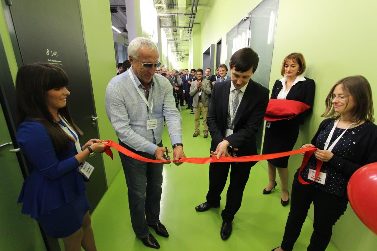
Researchers from Skoltech, Aalto University, and Peter the Great St.Petersburg Polytechnic University successfully demonstrated the technique for zinc oxide deposition on the surface of single-walled carbon nanotubes. The results of this collaboration have been recently published in Nanotechnology.
Single-walled carbon nanotubes (SWCNTs) – a cylindrical structure (with diameter of several nanometers and length of several microns), made of carbon atoms. SWCNTs have unique mechanical, electrical and optical properties that make them one of the most explored material in the world. Possible applications of SWCNTs include composite materials, supercapacitors, bio- and chemical sensors, transistor structures.
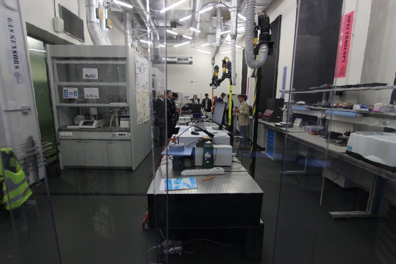
The use of pristine SWCNTs without their modification is limited in some areas, that’s why researchers are actively investigating all possibilities to change and improve properties of SWCNTs. In this study, researchers used method of SWCNTs treatment with nitrogen, developed at Skoltech Laboratory of Nanomaterials, and then coating the surface of carbon nanotubes with zinc oxide.
In this study, researchers achieved uniform zinc oxide (ZnO) coating by mean of atomic layer deposition (ALD), after the single-walled carbon nanotube (SWCNT) treatment in a controlled ozone atmosphere. Transmission electron microscopy (TEM) images of the SWCNTs after the treatment are shown in Figs. 1a and 1b. It can be clearly seen from Fig. 1a that deposition of ZnO is quite poor on the surface of the pristine nanotubes and leads to the formation of large particles. In contrast, Fig. 1b shows the ZnO coated sample exposed at ozone. The uniformity of ZnO coating in this case can be clearly observed.
Further treatment with ultraviolet of zinc oxide coated nanotubes led to their hydrophilic behavior (Fig. 2a and 2b). The hydrophobicity of the nanotubes prevents their application in different solutions, used, for example, in medicine and pharmacology, and their functionalization – making them hydrophilic – allows controlling their solubility.
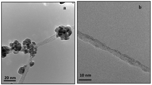
Fig. 1. a – TEM images of pristine SWCNT sample after 150 cycles of ALD without ozonization,
b – SWCNT after ozonization and coated with ZnO.
Moreover, the use of thin SWCNT films coated with ZnO allowed researchers to fabricate ambipolar transistors (with charge carriers “holes” and electrons) from p-type field-effect transistors (with “holes” as charge carriers). It is well known fact, that field effect transistors based on SWCNTs are p-type under normal ambient conditions (Fig. 2c), while by using zinc oxide deposition on SWCNTs scientists were able to change properties of transistor. “Here, we combine these two materials making ozone functionalized SWCNT TFTs coated with ALD ZnO and therefore tuning the electrical properties of the devices”, said coauthor Albert Nasibulin, a professor at the Skolkovo Institute of Science and Technology. “Unlike p-type transistors obtained under ambient conditions, our TFTs fabricated by ALD coating became ambipolar (Fig. 2d). This unique behavior has been a drawback in Si technology, in which only one type of charge carrier is dominant to operate the device. For this reason, demonstrated ambipolar SWCNT transistors coated with ZnO (50 cycles) could be easier utilized for logic circuit fabrication” continued Albert Nasibulin.
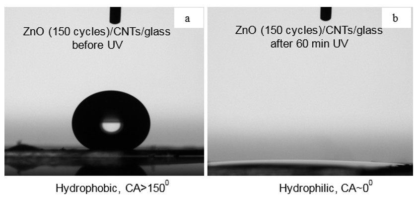
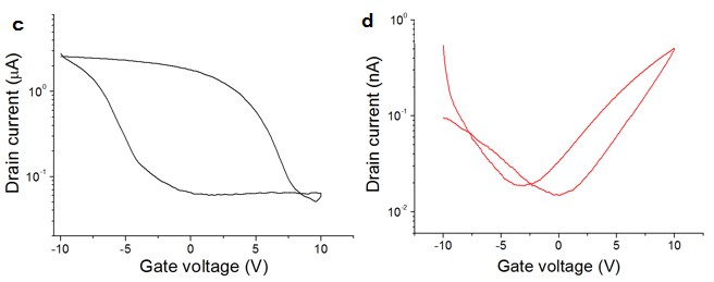
Fig. 2. Contact angle of water droplet a – before UV treatment, b – after UV treatment. IV characteristics of a SWCNT transistor on a logarithmic scale c – before ZnO ALD coating, d – after ALD coating.
The research group of Albert Nasibulin actively engaged in development of new nanomaterials and their applications. Among the recent achievements: development of carbon nanotubes treatment method with ozone, creation of novel hybrid material for touchscreen technology, creation of diodes based on SWCNTs, as well as stretchable supercapacitors based on SWCNTs.
The results of the study were published in Nanotechnology.
Contact information:
Skoltech Communications
+7 (495) 280 14 81